Background
The drift - diffusion system of equations for semiconductor devices is given by:
\begin{cases}
\nabla^2 \phi = \frac{q}{\varepsilon_s}(n - p - N_D^+ + N_A^-) & \text{(Poisson's equation, governing electric potential)} \\
\frac{\partial n}{\partial t} = \nabla \cdot ( \mu_n n \nabla \phi - D_n \nabla n ) + R(n,p) & \text{(Electron continuity equation)} \\
\frac{\partial p}{\partial t} = \nabla \cdot ( \mu_p p \nabla \phi + D_p \nabla p ) - R(n,p) & \text{(Hole continuity equation)}
\end{cases}
where \phi is the electric potential, n and p are electron and hole concentrations, \mu_n, \mu_p are electron and hole mobilities, D_n, D_p are diffusion coefficients, N_D^+ and N_A^- are ionized donor and acceptor concentrations, and R(n,p) is the recombination - generation rate.
The traditional current density formulas are:
- For electrons: J_n = -q\mu_n n \nabla \phi + qD_n \nabla n, combining drift -q\mu_n n \nabla \phi, driven by the electric field and diffusion qD_n \nabla n, driven by the concentration gradient.
- For holes: J_p = -q\mu_p p \nabla \phi - qD_p \nabla p, with drift (-q\mu_p p \nabla \phi) and diffusion (-qD_p \nabla p) components. Numerically discretizing these equations—especially managing nonlinearities—poses challenges, which the Scharfetter - Gummel scheme addresses.
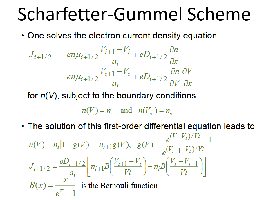
Scharfetter - Gummel Scheme
The Scharfetter - Gummel scheme discretizes current densities effectively. For example, the electron current density at a mid - point is:
\left.J_{n}\right|_{\text {mid }}=\frac{q V_{T} \mu_{n}}{\Delta x}\left[n_{i+1} B\left(\frac{\phi_{i+1}-\phi_{i}}{V_{t}}\right)-n_{i} B\left(\frac{\phi_{i}-\phi_{i+1}}{V_{t}}\right)\right]
This is only for 1D, also there are ways for 2D to get J_{nx} and J_{ny}
where B(x)=\frac{x}{e^{x}-1}, with limits like \lim _{x \rightarrow 0} B(x)=1 aiding in diverse physical scenarios.
Implementation Inquiry
I’m aiming to implement this Scharfetter - Gummel discretized current density in FEniCS. Has anyone done similar work? Specifically, how to code the B(x) function and handle element - across discretization in FEniCS? Any tips on managing nonlinear terms or mesh - related discretization would be awesome. Looking forward to your insights!
It is unclear to me the difficulty you are facing in defining B(x). Perhaps if you could make an attempt at writing the weak form it will help understand it. Nonetheless, why don’t you try this
B = lambda x: x/(ufl.exp(x)-1)
You can then use this function in your weak form as B((phi1-phi)/Vt)
I am only aware of Simudo as a complete implementation of DDR for semiconductor devices. You can refer to the associated publication for details about how they discretized the equations.
I should also warn that DDR equations formulated in terms of charge densities generally require very fine meshes at the pn interfaces. This could be very challenging in higher dimensions and will give a lot of headache with nonlinear convergence. It is better to use DDR in terms of energy as I think was done in Simudo.
Thank you for your quick reply. I’m sorry for my vague question just now. In the Scharfetter - Gummel Scheme discretization, the index “i” represents the spatial index rather than the temporal index. I’m wondering how to implement this discretization method in FEniCS. Yes, B(x) can indeed be implemented in this way, but my main question is still how to define the expression for this current density.
As for the simudo project. I have read this paper and unfortunately it did not imply the Scharfetter - Gummel Scheme discretization.
The details are at
Scharfetter - Gummel Scheme discretization
This kind of problem description is helpful when using the finite difference approach. You need to think how it will translate to the FEM way of describing problems which is to express the weak form. If you could get that then using first order lagrange elements will probably translate to the equations above.
To search if SG could be applicable to FEM, you might want to see this thesis and any follow up study. The research was later spun off into commercial program TiberCAD so if there is any merit in this approach then I presume they will have at least touched on it.
1 Like
Thank you very much. Through the link you provided, I found the process of SG-FEM simulation [1]. Generally speaking, compared with the Finite Volume Method (FVM), the Finite Element Method (FEM) may not be very suitable for semiconductor device simulation. There is a lot of relevant work that needs to adjust the FEM to make it adaptable to TCAD. Thank you again.
[1]G. . -L. Tan, X. . -L. Yuan, Q. . -M. Zhang, W. H. Ku and A. . -J. Shey, “Two-dimensional semiconductor device analysis based on new finite-element discretization employing the S-G scheme,” in IEEE Transactions on Computer-Aided Design of Integrated Circuits and Systems, vol. 8, no. 5, pp. 468-478, May 1989, doi: 10.1109/43.24875.
1 Like